导航

浏览

  • 首页
  • 中国国际半导体技术大会
  • 大讲堂
  • 招聘
首页 中国国际半导体技术大会 大讲堂 招聘
English
Richard Ali
  • 个人中心
  • Night mode
  • 退出
登录

账号密码登录

没有账号 去注册

找回密码

注册账号

已有账号 去登录

CSTIC预登记号登录

没有账号 去注册 账号密码登录

Symposium VII: Packaging and Assembly

Symposium VII: Packaging and Assembly

Virtual Conference Registration
  • Conference Agenda
  • CSTIC 2023 Call for Papers

Opening Remarks

  • Oral Session

  • Poster Session

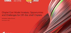
  • Chiplet Cost Model Analysis, Opportunities and Challenges for Off-the-shelf Chiplets

    Kaisheng Ma

    Tsinghua University

    Integration Strategy on Low-Cost Chip-First Fan-Out Panel Level Packaging

    Cheng-Tar Wu

    Chengdu ESWIN System IC Co., Ltd.

    Development and Application of Electroplating Copper Products with Low or Zero Internal Stress

    Peipei Dong

    Shinhao Materials LLC

    Design and Fabrication of High-Q IPDs for Process Design Kits on Glass Substrate

    Haozhe Ma

    Xiamen University

    Revent progress of laser induced TGV technology and it's applications

    Daquan Yu

    Xiamen University

    Investigation on Yield Improvement of Fan-out Wafer-level Packaging

    Kai Zhu

    ZTE Corporation

    Fine-pitch Cu-Sn transient-liquid-phase bonding based on reflow and pre-bonding

    Yunfan Shi

    Tsinghua University

    Flip Chip Thermal Stress Induced ILD Crack & Failure Analysis

    Suming Wang

    TF-AMD

    The study on warpage of epoxy molding compound

    Yangyang Duan

    Jiangsu HHCK Advanced Material Co. Ltd.

    Application of Single Wet equipment in WLP (Language: in Chinese)

    Yi Wang

    KINGSEMI

    State of the Art Metal Deposition System for Advanced UBM, RDL and Fan-Out Wafer Level Packaging

    Clinton Goh

    Applied Materials

    Laser Release Material for wafer level Fan-out Applications

    Guoping Zhang

    Shenzhen Institute of Advanced Electronic Materials

    Glass Carriers for Advanced Packaging

    James Li

    Corning Incorporated

    Dielectric property design based on BaTi2O5 nanorods and BaTiO3 nanoparticles couple and its application in embedded capacitor

    Wenzhong Zou

    School of Materials and Energy, University of Electronic Science and Technology of China

  • Optimization of Wafer Dicing-Saw to Reduce the Chipping Defect by using the Response Surface Methodology

    Hong Zhang

    Fudan University

    The research on small "dead zones" packaging technology for mass production of silicon photomultiplier

    Yuxiao Liu

    Beijing Normal University, collage of nuclear science and technology

    A SIMPLE METHOD FOR FINE VERTICAL INTERCONNECTION BY STENCIL PRINTED VIAS ON FLEXIBLE PRINTED CIRCUIT BOARD WITH LOW TEMPERATURE SINTERING NANO-SILVER PASTE

    Xiang Xun

    Institute of Semiconductors, Guangdong Academy of Sciences

Sponsors:

© 2022 SEMI 云官网. All Rights Reserved.

30