The fast changing and advancing scaling technique and potential device infrastructure

David Xiao
Shanghai Integrated Circuit Research and Develop (ICRD) Center

David Xiao
Shanghai Integrated Circuit Research and Develop (ICRD) Center
Richard Yang
Fortune Precision Corp, Shenyang


Douglas Guerrero
Brewer Science, Inc.
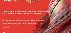
Qiang Wu
Fudan University
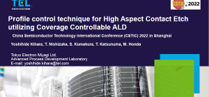
Yoshihide Kihara
TEL

Xing Ke
SMIC

Xing-Jun Yao
Beijing NAURA Microelectronics Equipment Co. Ltd
Zhiqiang Liu
AMEC

Vina Xu
AMEC
Dongming Zhou
AMEC


Shanyu Wang
Mattson


Li Tian Xu
Beijing NAURA Microelectronics Equipment Co. Ltd
Zengwen Hu
AMEC
Bo Su
Semiconductor Manufacturing International Corporation(SMIC)
Yuxin Yang
Leuven Instruments

Jun Wang
Semiconductor Manufacturing North China (Beijing) Corporation(SMNC)
Xiaohui Li
Naura


Yiming Zhang
Naura, China

Qiushi Xie
Beijing NAURA Microelectronics Equipment Co. Ltd

Zhu Chen
Shanghai University

Mimi Dai
Advanced Micro-Fabrication Equipment Inc. China

Chien-Pin Sherman HSU
Avantor
Xiaobing Liu
Shanghai IC R&D Center

Yiling Sun
Lam Research
Jie Yuan
Jiangsu Normal University
Chun Kai Wang
Lam Research

Li Fei Sun
Lam Research
Li Fei Sun
Lam Research

Caigan Chen
Lam Research
Bill Bian
Lam Research
Zhengning Li
Semiconductor Manufacturing International Corporation(SMIC)
Peng Yang
Shanghai IC R&D Center

Xu Jia
Lam Research

Tianhao Zhang
Lam Research
Hexin Zhou
Lam Research
PengFei Lyu
Lam Research

PengFei Lyu
Lam Research
Zhiyuan Xu
HLMC

Yajie Li
HLMC

Wenqiang Li
HLMC

Huang Shan
HLMC
Shaoxiong Liu
HLMC
Zheng Ruan
Lam Research
Rui Bao
Lam Research
Yujia Zhong
Lam Research
Julia Zheng
Lam Research
Jiajia Tian
Integrated Circuits Advanced Process R&D Center of IMECAS
Minxiang Wang
Lam Research
Jian Huang
Lam Research
Arthur Jin
Lam Research
Yingying Zhou
Lam Research

Swen Jin
Lam Research
YaQian Jiang
Lam Research

Junming Wang
Lam Research

Stan Zhang
Lam Research

Shanshan Nie
Lam research
Tao (McRee) Wang
Lam Research

Meng-Yu Xie
NAURA
Guang Yang
NAURA

Zheng Ji
NAURA

Hao Liu
NAURA
Hebao Liu
SMIC