导航

浏览

  • 首页
  • 中国国际半导体技术大会
  • 大讲堂
  • 招聘
首页 中国国际半导体技术大会 大讲堂 招聘
English
Richard Ali
  • 个人中心
  • Night mode
  • 退出
登录

账号密码登录

没有账号 去注册

找回密码

注册账号

已有账号 去登录

CSTIC预登记号登录

没有账号 去注册 账号密码登录

Symposium II: Lithography and Patterning

Symposium II: Lithography and Patterning

Virtual Conference Registration
  • Conference Agenda
  • CSTIC 2023 Call for Papers

Opening Remarks

  • Leo Pang

    D2S, Inc.

    View
  • Oral Session

  • Poster Session

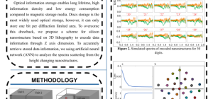
  • The fast changing and advancing scaling technique and potential device infrastructure

    David Xiao

    Shanghai Integrated Circuit Research and Develop (ICRD) Center

    3D NAND Technology Cost Scaling Challenges and Solutions

    Richard Yang

    Fortune Precision Corp, Shenyang

    Role of underlayers in novel patterning for EUV lithography

    Douglas Guerrero

    Brewer Science, Inc.

    Considerations in seting up industry standards for photolithography process, historical perspectives, methologies, and outlook

    Qiang Wu

    Fudan University

    The status of stochastic issues - Photon stochastic and Chemical Stochastic -

    TORU FUJIMORI

    FUJIFILM Corporation

    Advanced Lithography Material Status toward 5nm Node and beyond

    Koichi FUJIWARA

    JSR Shanghai Co., Ltd.

    Thickness Dependence of Properties of EUV Underlayer Thin Films

    Jae Hwan Sim

    DuPont Electronics and Industrial

    Process window, and process optimization in both Low and High NA EUV lithography for advanced logic technologies nodes

    Yanli Li

    Fudan University

    Critical pattern selection for full chip SMO application

    Sikun Li

    Shanghai Institute of Optics and Fine Mechanics

    Machine Learning Post Lithography Resist 3D Structure Model For Full Chip Implementation

    Xuelong Shi

    Shanghai IC R&D Center

    Inverse lithography technology: 30 years from concept to practical, full-chip reality

    Leo Pang

    D2S, Inc.

    Gan-based fast mask near-field calculation

    Yijiang Shen

    Guangdong University of Technology

    Model-driven Deep Learning for Computational Lithography

    Xu Ma

    Beijing Institute of Technology

    A Study of Improved Design Rules through Allowing 4degree Metal Lines

    Xianhe Liu

    Fudan University, School of Microelectronics

    High Power LPP-EUV Source for Semiconductor HVM Lithography and Other Application

    Hakaru Mizoguchi

    Gigaphoton

    Nanoimprint Performance Improvements for High Volume Semiconductor Manufacturing Keita Sakai

    Keita Sakai

    Canon Inc.

    EPE and CD performance enhancement by "GT66A", the next-generation immersion ArF lightsource

    Takamitsu Komaki

    Gigaphoton

    KrF Multi-Focal Imaging system for advanced and legacy applications

    Will Conley

    ASML

    Critical dimension metrology: from OCD to XCD

    Xiuguo Chen

    Huazhong University of Science and Technology

    A new generation cost-efficient laser mask writer, addressable up to the 90nm node

    Youngjin Park

    Mycronic Co., Ltd.

    EUV vacuum system safety while maximizing process productivity

    Zhen Ma

    Edwards

    DOSE CONTROL STRATEGY USING RANDOM LOGIC DEVICE PATTERNS AND MASSIVE METROLOGY IN A FOUNDRY HIGH VOLUME MANUFACTURING ENVIRONMENT (PPT)

    Kan Zhou

    HLMC

    Patterning capability of surface plasmon imaging

    Lihong Liu

    Institute of Microelectronics, Chinese Academy of Sciences

  • Utilizing Bossung Plot to calibrate OPC optical model

    Jian Wang

    Semiconductor Manufacturing International Corporation

    CD-SEM contour extraction for complex features measurement

    Ting He

    Semiconductor Manufacturing International (Shanghai) Corporation

    New model-rules-hybrid sbar placement strategy for 2D pattern

    Ge Zhang

    Semiconductor Manufacturing International Corporation

    Process Window Integration Rule Check for BEOL in Advanced Tech Node

    Xiaoyan Wang

    Semiconductor Manufacturing International Corporation(SMIC)

    Effect of high energy implantation on the photoresist for smaller size CMOS image sensor

    Chen Hui

    HLMC

    Stitching Process Development on 300mm Wafer CMOS BEOL for High Performance Chip Application

    Xiaoxu Kang

    Shanghai ICR&D Center

    Novel optical storage scheme with three recording dimensions enables a high density storage

    Dekun Yang

    Wuhan University

Sponsors:

© 2022 SEMI 云官网. All Rights Reserved.

30